The CY7C68001 stands as a USB microcontroller designed by Cypress Semiconductor, now Infineon. This chip features an 8-bit RISC CPU, USB 2.0 connectivity, and multiple I/O pins, making it a strong choice for anyone interested in electronics. Many students begin their electronics journey by exploring a project that uses a CY7C68001 Circuit Diagram. Understanding these diagrams helps beginners build confidence as they start their first project, whether for industrial automation, automotive, or a classroom tutorial. Each project offers hands-on experience with real-world applications, leading to better skills with every new project.
Key Takeaways
-
The CY7C68001 is a USB 2.0 controller chip ideal for beginners and professionals working on embedded systems and USB projects.
-
Understanding and reading the CY7C68001 circuit diagram helps build confidence and skills in electronics by showing how components connect and work together.
-
Each pin on the CY7C68001 has a specific function; knowing these helps design reliable circuits and avoid wiring mistakes.
-
Using the official datasheet is essential for accurate information on pinouts, power requirements, and example circuits to guide project building.
-
The CY7C68001 supports many applications like USB data loggers and USB-to-parallel converters, making it a versatile choice for learning and real-world projects.
Overview
What Is CY7C68001
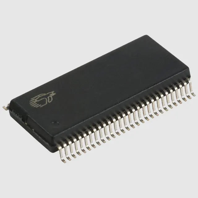
The CY7C68001 is a USB 2.0 bus controller designed by Cypress Semiconductor. This device belongs to the EZ-USB SX2™ family and uses CMOS technology. It features a parallel interface, which allows it to connect with microprocessors, DSPs, ASICs, and FPGAs. The chip operates at a voltage range of 3V to 3.6V and comes in a 56-pin SSOP package. The main function of the CY7C68001 is to manage high-speed USB communication between a host and various devices. Many engineers use this controller in embedded systems, consumer electronics, and industrial automation. Students often choose this chip for their first project because it offers reliable performance and supports a wide range of applications.
| Attribute | Description |
|---|---|
| Device Name | CY7C68001-56PVXC |
| Function | USB 2.0 Bus Controller |
| Architecture | USB controller with parallel interface |
| Package | 56-SSOP |
| Technology | CMOS |
| Family | EZ-USB SX2™ |
| Operating Voltage | 3V to 3.6V |
| Features | Auto flow control, false start bit detection |
| Status | Obsolete |
Key Features
The CY7C68001 offers several important features that make it suitable for many types of project.
-
USB 2.0 certified, supporting both high-speed (480 Mbps) and full-speed (12 Mbps) operation
-
Four configurable endpoints with a shared 4 KB FIFO buffer, plus a control endpoint for device requests
-
Standard 8- or 16-bit external master interface, compatible with many processors and FPGAs
-
Integrated phase-locked loop (PLL) for stable clock generation
-
Operates at 3.3V, with 5V tolerant input/output pins
-
Available in 56-pin SSOP and QFN packages
-
Moisture Sensitivity Level 3 (168 hours), suitable for various environments
-
Supports applications such as DSL modems, memory card readers, cameras, scanners, wireless LAN, MP3 players, networking, and printers
Tip: Beginners can use the CY7C68001 in a project like a USB data logger or a simple USB-to-parallel converter. These projects help students learn about USB communication and device interfacing.
The chip’s flexibility and broad compatibility make it a popular choice for both classroom and industrial project work. Its robust design ensures that each project can handle fast and secure data transfer, which is essential for modern electronics.
CY7C68001 Circuit Diagram
Schematic Basics
A schematic diagram shows how electronic components connect in a circuit. The cy7c68001 circuit diagram uses standard symbols to represent each part. These symbols help everyone understand the design, no matter where they live or work. For example, a resistor appears as a zigzag line, while a capacitor looks like two parallel lines. The cy7c68001 circuit diagram often includes symbols for resistors, capacitors, diodes, transistors, crystals, and integrated circuits. Each component has a unique name, such as R1 for a resistor or U1 for the cy7c68001 chip. The value, like resistance in ohms or capacitance in farads, appears next to the symbol.
Note: The datasheet from Cypress Semiconductor provides official schematic examples and detailed information about the cy7c68001 circuit diagram. Beginners should always check the datasheet before starting a new project.
Component names use letter prefixes:
-
R for resistors
-
C for capacitors
-
U for integrated circuits (like the cy7c68001)
-
L for inductors
-
D for diodes
-
Q for transistors
-
Y for crystals
Wires connect the components. Where wires meet, a dot shows a connection. Sometimes, designers use net names instead of drawing every wire. This method keeps the cy7c68001 circuit diagram clean and easy to read. Special symbols exist for parts like fuses, logic gates, voltage regulators, and connectors. The cy7c68001 appears as a rectangle with labeled pins, showing how it connects to other parts of the project.
There are several types of diagrams:
-
Schematic diagrams: Show the electrical connections and functions. Most cy7c68001 circuit diagram examples use this type.
-
Wiring diagrams: Focus on physical layout and wire routing.
-
Block diagrams: Show the main sections of a system.
-
Pictorial diagrams: Use images instead of symbols.
For most embedded projects, schematic diagrams give the clearest view of how the cy7c68001 connects to other devices.
How to Read
Reading a cy7c68001 circuit diagram starts with finding the main chip, usually labeled U1. The pins on the cy7c68001 connect to other components, such as resistors, capacitors, and connectors. Each pin has a specific function, which the datasheet explains in detail. Beginners should follow the signal flow, starting at the USB connector and tracing the path through the cy7c68001 to the output devices.
Best practices for reading and drawing cy7c68001 circuit diagrams include:
-
Use standard symbols and naming conventions.
-
Start with simple circuits before moving to complex designs.
-
Follow the signal flow from input to output.
-
Label all nets and components clearly.
-
Check the datasheet for correct pin connections and values.
Tip: Beginners can use free circuit diagram software, such as KiCad or EasyEDA, to draw and edit their own cy7c68001 circuit diagram. Practicing with breadboards helps students test their project before soldering components.
A good cy7c68001 circuit diagram makes it easier to build and troubleshoot an embedded project. Students often start with a simple USB-to-parallel converter or a data logger as a first project. These projects help them learn how to read diagrams, connect components, and understand how the cy7c68001 works in an embedded system. A step-by-step tutorial can guide beginners through each stage, from reading the diagram to building the final project.
Pinout
Pin Diagram
The CY7C68001 comes in a 56-pin SSOP package. Each pin has a unique role in the circuit. The pin diagram shows the physical layout of the pins around the chip. This diagram helps students and engineers connect the chip correctly in a project. Most datasheets include a top-view image that labels each pin with its number and function. For the CY7C68001, the diagram usually places pin 1 at the top left corner. The numbers increase counterclockwise around the chip.
Here is a simplified example of how a pin diagram might look:
         +-----------------------------+
     1  |                             | 56
     2  |                             | 55
     3  |                             | 54
    ... |        CY7C68001            | ...
    28  |                             | 29
         +-----------------------------+
Tip: Always check the official datasheet for the exact pin diagram before starting a project. This step prevents wiring mistakes and saves time during troubleshooting.
Pin Functions
Each pin on the CY7C68001 serves a specific function. Some pins handle power, while others manage data or control signals. Understanding these roles helps users design a reliable project.
Common pin functions include:
-
VCC: Supplies power to the chip.
-
GND: Connects to ground.
-
USB D+ / D-: Handle USB data signals.
-
CLKOUT: Provides a clock signal for other parts of the project.
-
FIFO Data Lines (FD0–FD15): Transfer data between the chip and external devices.
-
Control Pins (SLRD, SLWR, SLOE, etc.): Manage data flow and timing.
-
RESET: Resets the chip during startup or troubleshooting.
A table helps summarize the main pin functions:
| Pin Name | Function |
|---|---|
| VCC | Power supply |
| GND | Ground |
| D+ / D- | USB data lines |
| FD0–FD15 | Data bus for external devices |
| SLRD | FIFO read control |
| SLWR | FIFO write control |
| SLOE | FIFO output enable |
| CLKOUT | Clock output |
| RESET | Chip reset |
When building a project, users should match each pin to its correct connection. Careful planning ensures the project works as expected. Beginners often start with simple connections, then expand their project as they gain confidence.
Datasheet
Where to Find
Anyone starting a project with the CY7C68001 should begin by finding the official datasheet. Cypress Semiconductor, now part of Infineon, provides the datasheet on its website. Many trusted electronics distributors, such as Digi-Key and Mouser, also offer downloadable datasheets. Searching for "CY7C68001 datasheet PDF" in a search engine often leads directly to the correct document. The datasheet usually appears as a PDF file. It contains all technical details, pin diagrams, and application notes. Beginners should always use the latest version to ensure accurate information.
Tip: Always download datasheets from official or reputable sources to avoid outdated or incorrect information.
How to Use
The datasheet serves as a roadmap for understanding and using the CY7C68001. Beginners should focus on several key sections to build a strong foundation:
-
The Function section describes the chip’s main job as a USB controller and explains how it fits into electronic circuits.
-
The Interface section shows how the device connects to other systems, including details about the parallel interface and USB 2.0 protocol.
-
The Operating Supply Current and Supply Voltage sections list the power needs, which helps users design safe and reliable circuits.
-
The Clock Frequency and Data Rate sections set the limits for speed and performance.
-
The Protocol and Standards sections explain the rules for communication and confirm that the chip meets USB 2.0 requirements.
-
The Endpoints and FIFO memory sections describe how the chip handles and stores data.
-
The Reference Designs section provides example circuits, firmware, and extra documentation. These resources help beginners learn by example.
A table can help organize these important sections:
| Section Name | Why It Matters for Beginners |
|---|---|
| Function | Explains the chip’s main role |
| Interface | Shows how to connect the chip |
| Supply Current/Voltage | Lists power requirements |
| Clock/Data Rate | Sets speed and performance limits |
| Protocol/Standards | Ensures communication compatibility |
| Endpoints/FIFO | Details data handling |
| Reference Designs | Offers practical examples |
Reading the datasheet step by step helps beginners avoid mistakes and design better projects.
Equivalents and Uses
Equivalent ICs
Many engineers look for alternatives to the CY7C68001 when planning a project. Several USB microcontrollers from other manufacturers offer similar features. The FTDI FT232 series, Microchip PIC USB microcontrollers, and Silicon Labs CP210x series often serve as equivalents. These chips support USB communication and work well in embedded systems. Each option has unique strengths, so users should compare them before choosing one for their project design.
The table below highlights the main features of the CY7C68001 and its equivalents:
| Feature/Attribute | CY7C68001-56PVXC Details |
|---|---|
| Core Architecture | Enhanced 8051-compatible microcontroller |
| USB Compliance | USB 2.0, supports high-speed (480 Mbps) and full-speed |
| Memory | 8 KB to 16 KB on-chip RAM |
| Package Type | 56-pin QFN or SSOP |
| Operating Voltage | 3.0 V to 3.6 V |
| Operating Temperature Range | 0°C to 70°C (some sources mention -40°C to +85°C) |
| Interfaces | Parallel interface, I2C, SPI, UART |
| Power Consumption | Approx. 200 mA |
| Additional Features | In-system programming, multiple I/O ports, timers, DMA |
| Equivalent Products | FTDI FT232, Microchip PIC USB, Silicon Labs CP210x |
Note: The FTDI FT232 series works best for simple USB-to-serial interfacing. Microchip PIC USB microcontrollers fit well in custom embedded project design. Silicon Labs CP210x series offers easy integration for USB-to-UART projects.
Applications
The CY7C68001 finds use in many embedded projects. Students and engineers often choose this chip for USB data loggers, USB-to-parallel converters, and device programmers. These projects help beginners learn about USB communication and interfacing with other devices. The chip’s parallel interface makes it easy to connect with FPGAs, microprocessors, or sensors in a project.
Common uses include:
-
Building a USB data logger for recording sensor data in a science project.
-
Creating a USB-to-parallel converter for controlling older printers or devices.
-
Designing a device programmer for embedded development boards.
-
Developing a custom USB interface for robotics or automation projects.
Tip: Beginners can start with a simple USB-to-parallel converter project. This project teaches the basics of USB communication, embedded system design, and safe interfacing.
Many classroom activities use the CY7C68001 to teach embedded concepts. The chip’s flexibility allows students to experiment with different project design ideas. Each project helps users gain hands-on experience with real-world interfacing and embedded systems.
Understanding the CY7C68001 helps students and engineers build a strong foundation for any project. Key points include high-speed USB 2.0 support, energy efficiency, flexible interfaces, and reliable operation in many project types.
-
The chip’s built-in FIFO memory and enhanced microcontroller core make it ideal for project designs in embedded systems, consumer electronics, and automation.
-
Practicing with schematics and breadboards strengthens project skills.
-
Online tutorials, datasheets, and free circuit drawing tools support learning for every project.
-
Building simple circuits and studying symbols prepare users for more advanced project work.
-
Using resources like SparkFun and JLCPCB blogs helps users understand schematic flow for each project.
-
Creating and testing circuits on breadboards gives hands-on experience for any project.
-
Exploring series and parallel circuits improves project understanding.
-
Referencing datasheets ensures correct connections in every project.
-
Tutorials on schematic symbols and drawing help users start a project with confidence.
-
Each project offers a chance to learn, experiment, and grow as an electronics builder.
Keep practicing and experimenting with each project. Every new project brings valuable skills and deeper knowledge of the CY7C68001.
FAQ
What is the main use of the CY7C68001?
The CY7C68001 acts as a USB 2.0 controller. Engineers use it to connect devices to computers or other hosts. It works well in data loggers, USB converters, and device programmers.
Can beginners use the CY7C68001 for simple projects?
Yes. Many students start with this chip. They often build USB-to-parallel converters or data loggers. The chip’s datasheet and example circuits help beginners learn step by step.
Where can someone find example circuits for the CY7C68001?
Most datasheets include reference designs. Electronics websites like SparkFun and JLCPCB also share sample circuits. These resources help users understand how to connect and use the chip.
What should someone do if the CY7C68001 circuit does not work?
-
Check all connections against the schematic.
-
Make sure the power supply matches the chip’s needs.
-
Review the datasheet for correct pin usage.
-
Test the circuit on a breadboard before soldering.
Written by Jack Elliott from AIChipLink.
AIChipLink, one of the fastest-growing global independent electronic components distributors in the world, offers millions of products from thousands of manufacturers, and many of our in-stock parts is available to ship same day.
We mainly source and distribute integrated circuit (IC) products of brands such as Broadcom, Microchip, Texas Instruments, Infineon, NXP, Analog Devices, Qualcomm, Intel, etc., which are widely used in communication & network, telecom, industrial control, new energy and automotive electronics.
Empowered by AI, Linked to the Future. Get started on AIChipLink.com and submit your RFQ online today!


